Solar cells
We carry out search for third generation solar cells. Particularly, we seek and characterize such materials where thin-film or nanostructured semiconductors may show enhanced absorption and/or carrier multiplication for increased efficiency.
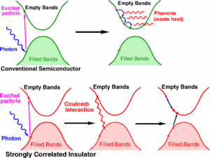
In collaboration with Manousakis group at Florida State University, we propose<bib id="PhysRevB.90.165142"/> that strongly correlated materials are strong candidates for realizing efficient photovoltaic cells because the enhanced carrier multiplication rates. The idea is sketched on the figure.
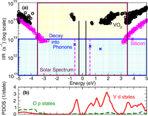
We have shown by first-principles calculations that the carrier multiplication rate is two orders of magnitude higher in VO2 than in Si and much higher than the rate of hot electron/hole decay due to phonons. As VO2 is a proto-typical material of strongly correlated materials, we think that the family of strongly correlated materials exhibit similar properties. This may lead to a single photon in - two electrons out operation of solar cells in strongly correlated materials that can significantly increase the efficiency of this type solar cells compared to the case of conventional semiconductors. <bib id="PhysRevB.90.165142"/>
Characterization of an efficient light absorber: point defects in tin monosulfide (SnS)
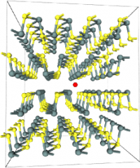
Tin monosulfide (SnS) is quasi-2D material which is a metastable crystalline form of Sn and S. From solar cell application point of view, the very attractive property of SnS is the strong absorption starting at about 1.3 eV. However, the real SnS material is very defective, and often exhibits unintentional p-type doping. In collaboration with Kaxiras group at Harvard University we found<bib id="malone2014first" /> that for the intrinsic defect, Sn-vacancy acceptor defect is responsible for the intrinsic p-type conductivity of SnS. For the extrinsic defects, we find support for the experimental suggestion that P, under S-rich conditions, prefers to substitutionally occupy the Sn site rather than the S site, and this leads to n-type behavior. Additionally, we support that Sb acts as a donor in Sn. We also show that Cl prefers to substitute for S atoms where it acts as a donor.
Enhanced absorption and carrier multiplication in semiconductor nanoparticles
Surface effects on nanoparticle boundaries in solid-state matrix can help circumvent the limitations of traditional (first and second-generation) photovoltaics. This effect may be enhanced and fine-tuned by modifying the surface. The core aim of this strategy is to produce solid-state systems which absorb visible light, and in which the resulting high-energy exciton generates multiple charge carriers instead of decaying into a low-energy one by heating the solar cells.
Tweaking the absorption of Si nanoparticles by surface engineering
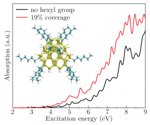
We calculated ab-initio the absorption of Si nanoparticles with various surface terminations <bib id='PhysRevB.87.155402' />, <bib id='doi:10.1021/nl901970u' />. We showed in collaboration with Giulia Galli group at UC Davis that the surface termination of small nanoparticles can seriously change their absorption spectrum in the lowest energy region which can be the most critical in solar cell applications. In addition, we showed that the empty states of the nearby Si nanoparticles interact with each other that also seriously influence their absorption properties <bib id='doi:10.1021/nl901970u' />. This finding explains previous experimental data on colloid quantum dots, and highlighted the importance of surface engineering and the role of the density of nanoparticles towards the optimization for solar cell applications.
Solution to the quantum confinement dilemma: enhanced carrier multiplication rates in the solar spectrum in Si and Ge metastable nanoparticles
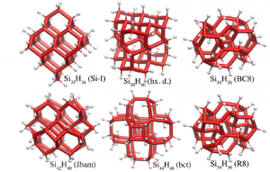
Multiple Exciton Generation (MEG) in nanoparticle-based solar cells promises to increase the cell-efficiency above the Shockley–Queisser limit. However, utilizing MEG is hampered by the Quantum Confinement Dilemma (QCD): quantum confinement advantageously increases the effective Coulomb interaction, but at the same time disadvantageously increases the electronic gap. Using ab initio calculations we showed in collaboration with Giulia Galli group at UC Davis that germanium nanoparticles with core structures of high pressure phases of bulk Ge can transcend the QCD, by simultaneously lowering gaps and increasing the MEG rates above those of NPs with a cubic diamond core. Synthesis routes to obtain Ge colloidal ST12 core structures are available and hence we propose that exploring ST12 Ge NPs for MEG solar cells is a promising research effort <bib id="C4TA01543F"/>. We also showed that Si nanoparticles with a BC8 core structure exhibit significantly lower optical gaps and MEG thresholds, and an order of magnitude higher MEG rate than diamondlike ones of the same size <bib id="PhysRevLett.110.046804"/>. This BC8 phase of Si can be fabricated by various techniques, thus our proposal opens the window for efficient solar cell absorbers from environment friendly and widely accessible materials and materials processing.
Efficient electron-hole separation for Si nanoparticles embedded into a matrix
Solar cell application of the very promising silicon or germanium nanoparticles (NP) requires such a matrix where the photo-generated carriers can be efficiently separated and can be lifted to the contacts. The strong Coulomb interaction between the carriers in nanoparticles mediate the MEG process, however, this strong Coulomb interaction may also disadvantageously inhibit the efficient separation of the two types of carriers, electrons and holes, needed for photo-voltaics operation.
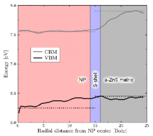
We propose that embedding silicon NP into amorphous, nonstoichiometric zinc-sulfide (ZnS) leads to promising nanocomposites for solar energy conversion. Using ab initio molecular dynamics simulations we show in collaboration with Giulia Galli group that, upon high temperature amorphization of the host chalcogenide, sulfur atoms are drawn to the NP surface. We find that the sulfur content may be engineered to form a type II heterojunction, with complementary charge transport channels for electrons and holes, and that sulfur capping is beneficial to lower the nanoparticle gap, with respect to that of NPs embedded in oxide matrices <bib id='PhysRevLett.112.106801' />.
Bibliography
<biblist />
