Solar cells
We carry out search for third generation solar cells. Particularly, we seek and characterize such materials where thin-film or nanostructured semiconductors may show enhanced absorption and/or carrier multiplication for increased efficiency.
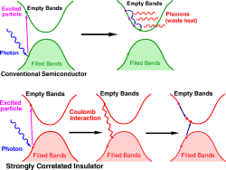
In collaboration with Manousakis group at Florida State University, we propose that strongly correlated materials are strong candidates for realizing efficient photovoltaic cells because the enhanced carrier multiplication rates. The idea is sketched on the figure.
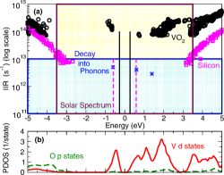
We have shown by first-principles calculations that the carrier multiplication rate is two orders of magnitude higher in VO2 than in Si and much higher than the rate of hot electron/hole decay due to phonons. As VO2 is a proto-typical material of strongly correlated materials, we think that the family of strongly correlated materials exhibit similar properties. This may lead to a single photon in - two electrons out operation of solar cells in strongly correlated materials that can significantly increase the efficiency of this type solar cells compared to the case of conventional semiconductors.
Physical Review B 90 165142 (2014) DOI:10.1103/PhysRevB.90.165142
Characterization of an efficient light absorber: point defects in tin monosulfide (SnS)
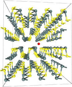
Tin monosulfide (SnS) is quasi-2D material which is a metastable crystalline form of Sn and S. From solar cell application point of view, the very attractive property of SnS is the strong absorption starting at about 1.3 eV. However, the real SnS material is very defective, and often exhibits unintentional p-type doping. In collaboration with Kaxiras group at Harvard University we found that for the intrinsic defect, Sn-vacancy acceptor defect is responsible for the intrinsic p-type conductivity of SnS. For the extrinsic defects, we find support for the experimental suggestion that P, under S-rich conditions, prefers to substitutionally occupy the Sn site rather than the S site, and this leads to n-type behavior. Additionally, we support that Sb acts as a donor in Sn. We also show that Cl prefers to substitute for S atoms where it acts as a donor.
Phys. Chem. Chem. Phys. on-line (2014). DOI:10.1039/C4CP03010A


