Defect Identification
Part of our research is devoted to the characterisation of paramagnetic colour centres by providing insight into their electronic structure. We focus on different types of materials to be used as hosts for the defects. All of them are relevant in present-day technology and among them diamond and silicon carbide play the major role.
The remarkable properties of diamond, combined with the possibility to exploit some of its point defects as quantum bits in quantum information processing or as emitters in biomarkers, make this system extremely attractive for applications. On the other hand, silicon carbide is characterised by a wealth of defects with many important properties and moreover, it is acquiring increasing importance as a host, given the technology already associated to it and ready to be exploited.
Defect identification in general is based on a combination of experiment and theory complementing each other. Experiments point towards the realisation of the actual device while theoretical results can serve as a guide given the precision by which models can be built. Most of the works resulted in joint papers appeared in Physical Review B, Applied Physics Letters and Physical Review Letters in the last 10 years.
The outcomes of our research are based on DFT calculations which are an invaluable and faithful tool for calculating the properties of matter. By means of DFT we provide structural data, formation energies and optical properties of defects in solids and in nanostructures. The most successful identifications were based on the accurate calculation of hyperfine tensors and local vibration modes that can be compared to detected EPR and PL centres. In the following a few examples are illustrated.
Point defects in diamond
N2V defect in diamond
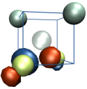
The exceptional perspectives of using the NV- centre in diamond as a quantum bit have triggered the search for other colour centres with similar or even better qualities. The properties that make this centre particularly interesting for quantum computing are connected to the presence of a paramagnetic ground state with long coherence times and spin levels that can be initialised by optical excitation and manipulated by microwaves at room temperature. Given the special nature of its transitions, the N2V defect centre shows marked resemblances to NV- and therefore may represent an alternative candidate for quantum technology applications. It is also known as H3 photoluminescence centre and it is constituted by two carbon and two nitrogen atoms connected to a vacancy (as shown in the figure on the left). By means of DFT calculations, we are currently working on the characterisation of the optical and magnetic properties of a single such centre embedded in diamond. Our experimental partners are engaged in photoluminescence and ODMR measurements.
Divacancy (V2) in diamond
Ion implantation is of core importance for engineering defects in diamond. For example, a class of applications that require implantation are those related to sensing. In that case, the probe centre (usually NV-) has to be created just beneath the diamond surface in order to enhance its detection capabilities. Unfortunately, as a by-product, implantation by irradiation creates vacancies and other defects that can be found within the hosting diamond matrix even after annealing. In this context, it has been shown that the divacancy defect (V2) forms with the highest probability <bib id="Deak2014"/>. V2 in diamond is constituted by two missing carbon atoms in adjacent positions. It also carries a spin and can therefore be the source of magnetic noise, moreover, it can absorb light at the energies applied for exciting other defects (for example NV-), thus causing unwanted spectral diffusion in their luminescence spectra. Given these premises, it is of primary importance to understand the optical and magnetic properties of this colour centre in order to optimise the conditions for implantation.
Silicon-Vacancy in diamond (SiV0 and SiV-)
Silicon in diamond is a common defect in CVD (chemical vapour decomposition) diamonds grown on silicon substrate.
The silicon vacancy defect in its neutral charge state has high spin state S=1, and its assigned to the KUL1 EPR signal. This interpretation has been evinced by hyperfine tensor calculated by ab-initio DFT with LDA <bib id="Goss2007"/>, and HSE06<bib id="gali2013ab"/> kernel for SiV gives a relatively good agreement with the experimental data<bib id="Edmonds2008"/> of the KUL1 EPR signal. These KUL3 EPR, and a 1.31eV PL signal were found out correlate <bib id="Haenens2011" /> with KUL1 (SiV0).
A PL(photoluminscence) center at 1.68eV with fine structure divided into 12 lines, which can be divided into 3 similar groups, containing 4 components. The ratio of these signals coincided with the natural abundances of silicon isotopes, such as 28Si, 29Si, and 30Si <bib id="Clark1995"/>, thus the underlying point defect must be silicon related. We have evinced that this 1.68eV line originates from the negatively charged silicon-vacancy. Our contrained DFT results are good agreement (1.72eV<bib id="gali2013ab"/>) with the experimental 1.68eV observation. With our method, the fine structure of SiV- has been also modeled. A weak near infrared absorption signal at 1.51eV<bib id="Neu2012" /> has been reported and assigned to SiV, our model gives 1.59eV<bib id="gali2013ab"/> electronic transition energy which is good agreement with the experimental results.
Point defects in silicon carbide
Carbon antisite-vacancy pair in silicon carbide
Vacancies are one of the most simple and fundamental point defects in crystals. However, in a compound material, the vacancies are not simple defects, as is generally expected. For instance, in an AB compound material, during the diffusion of the A vacancy one of its nearest neighbors, a B atom, can move into the vacant lattice site forming a pair of a B antisite and a B vacancy. The antisite-vacancy (AV) pairs are the counterpart of the isolated vacancies in compound materials, and can be energetically stable or metastable defects with respect to the vacancies.
The stability order of the cation vacancies and their anion AV counterparts depends on the Fermi level (EF): in p-type material, the anion AV complex is more stable than the cation vacancy, whereas in n-type material the cation vacancy is more stable. For a certain EF position both configurations are equally stable. Mutual transformations of AV complex and the cation vacancy can then be induced, e.g., when irradiation induced compensation centers anneal out and change the EF position. In this sense, the cation vacancy and the anion AV counterparts form a bistable defect pair.
In our knowledge, we firstly identified the fundamental AV defect in a compound semiconductor, namely, the negatively charged carbon AV defect in 4H-SiC as the SI5 EPR center in 4H-SiC. We also showed that this complex is an important compensating center in high purity semi-insulating SiC samples with acceptor levels at around 1.1 eV below the conduction band edge {{#btref: Umeda2006}}. There are indications that these type of AV defect may exist in III-V semiconductors, too.
Divacancy
Divacancies are common defects in semiconductors comprised of neighboring isolated vacancies. We could unambiguously identify the neutral divacancy in silicon carbide by a combined EPR/theory study. We applied DFT calculations to determine the geometry, the spin state and the hyperfine tensors of this defect <bib id="Son2006"/>. We found that the neutral divacancy has a high spin, S=1, state in its ground state and it is a very stable defect.
Peculiar hydrogen bonds
We investigated the hydrogen in silicon carbide by DFT supercell calculations. We found that hydrogen forms a three-center bond in the carbon vacancy <bib id="Gali2000"/>. The hydrogen in three-center bond does not passivate the dangling bonds but it possesses a donor character. Our findings attracted a great interest when metallic behavior of SiC surfaces was found by special hydrogen treatments <bib id="Chang2005"/>.
We investigated the possible occurance of the three-center bond of hydrogen in the anion vacancy of the partially polarized III-N semiconductors by DFT supercell calculations in order to sketch a general trend <bib id="Szucs2003"/>. We found that the behavior of hydrogen in the anion vacancy in compound semiconductors depends on two key parameters: (i) the ratio of the second-neighbor distance in the semiconductor to the ideal bonding distance between the cations and (ii) the ratio of the former to the ideal bonding distance between hydrogen and the cation. If the cation-cation distance in one semiconductor is comparable to twice the cation-hydrogen distance, the necessary condition for forming a three-center bond is established. If the ideal bonding distance between the cations is much less than the second-neighbor distance in the semiconductor then the cations will relax outward and the hydrogen will form a twocenter bond with one of them. The sufficient condition for the three-center bond is that the second-neighbor distance in the semiconductor be close to the ideal cation-cation bond length. The geometry of the X-H-X bridge depends on the difference in the electronegativities. Formation of two X-H-X bridges seems to prevent trapping of further hydrogen atoms in the vacancy which, therefore, remains electrically active upon hydrogenation.
Point defects in wurtzite aluminum nitride
Aluminum nitride (AlN) is a wide band gap semiconductor. Its wurtzite phase has a direct band gap of 6.12 eV that make it possible deep UV optoelectronic applications. Beside this it is used as a dielectric layer in optical data medium, electronic wafer, chip carrier, where the good thermal conduction is essential.
Group-II acceptors
Light-emitting diode (LED) made from Si and Mg doped AlN demonstrated to emit at short wavelength (210 nm) <bib id="Taniyasu2006"/>. The quantum efficiency of this emittance is low, due to the relatively low hole concentration (1012 cm−3 at room temperature in Mg-doped AlN). Therefore the understanding of the possible shallow acceptor levels, created by dopants and finding the one with the lowest thermal ionization energy is a key for the high efficiency UV LED source. We investigated the Al substitutional defects with the following group-II elements: Be, Mg, Ca, Sr, and Ba. Our findings showed that Be substitutional is not an effective masslike shallow acceptor, contrary to earlier findings <bib id="Wu2007"/>, Mg is the shallowest isolated group-II substitutional defect and Mg–O–Mg is even shallower acceptor than Mg <bib id="Szabo2010"/>.
Defects at nitrogen site
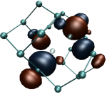
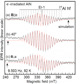
Doping of AlN is a serious problem because doping efficiency is significantly decreased by carrier compensation. Deep level defects such as residual oxygen at N site (ON) , and/or the N vacancy (VN) donor centers probably responsible for carrier compensation in the case of p-type doping. Similarly, Al vacancy acceptor center (VAl) probably responsible for carrier compensation in the case of n-type doping. To the best of our knowledge we identified in the first time the VN donor center, comparing the results of electron paramagnetic resonance (EPR) measurement and ab initio supercell calculation. We found that the specific EPR spectrum was only observed after electron irradiation, therefore the associated defect is likely to be intrinsic. The EPR spectrum showed a clear hf structure due to the interaction with four nearest Al neighbors. Ab initio calculation showed ground state with a distorted neighborhood around the vacant site, possessing C1h symmetry. Spin density distribution among the four Al-atoms near the vacant site found to be almost equal, fitting well with the measured EPR spectrum. Based on the good agreement in the hf parameters estimated from EPR and obtained from ab initio supercell calculations, we suggested the measured defect to be the best candidate for the neutral N vacancy in AlN <bib id="Son2011"/>.
Nitrogen split interstitial
Recent finding in wurtzite gallium nitride (GaN) <bib id="Bardeleben2012" /> motivated the research to investigate the nitrogen spit interstitial defect in AlN. We carried out Heyd-Scuseria-Ernzerhof hybrid density functional theory plane wave supercell calculations in wurtzite aluminum nitride in order to characterize the geometry, formation energies, transition levels, and hyperfine tensors of this defect. The calculated hyperfine tensors may provide useful fingerprint of this defect for electron paramagnetic resonance measurement <bib id="Szallas2014"/>.
Bibliography
<biblist />


